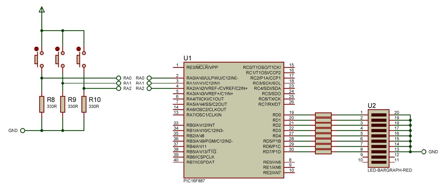
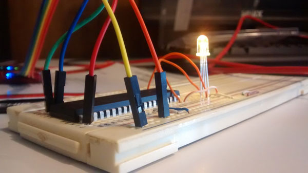
El siguiente diagrama muestra el circuito básico a utilizar
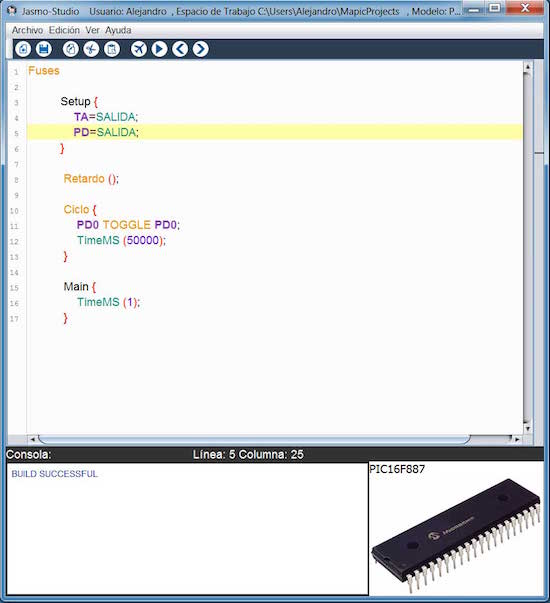
       Fuses

          Setup {
              TA=SALIDA;
              PD=SALIDA;
          }

           Retardo ();

           Ciclo {
               PD0 TOGGLE PD0;
               TimeMS (50000);
           }

           Main {
               TimeMS (1);
           }
Al crear un proyecto en Jasmo Studio , se crea una carpeta y dentro de ella el archivo, con extensión .mapic
En Jasmo Studio , se presenta el código , a compilar , como se muestra a continuación.
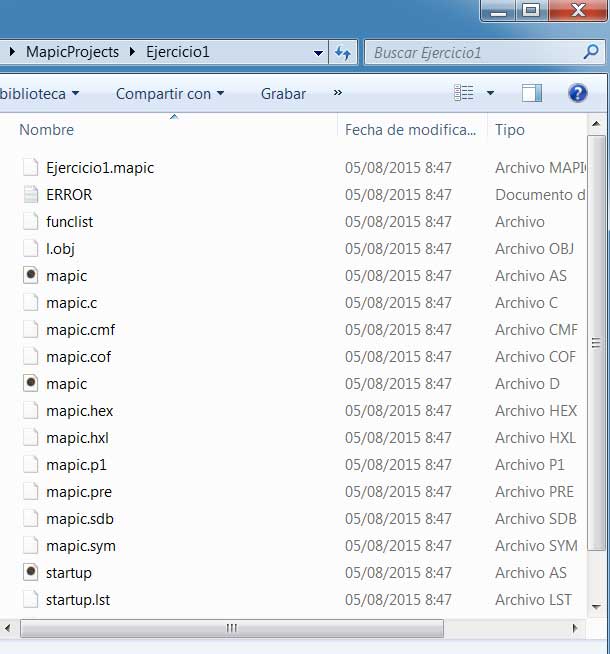
Al Compilar el archivo , en la carpeta del proyecto se crean los archivos correspondientes.
#include <xc.h>
// CONFIG1
#pragma config FOSC = INTRC_NOCLKOUT
#pragma config WDTE = OFF
#pragma config PWRTE = OFF
#pragma config MCLRE = OFF
#pragma config CP = OFF
#pragma config CPD = OFF
#pragma config BOREN = OFF
#pragma config IESO = OFF
#pragma config FCMEN = OFF
#pragma config LVP = OFF


// CONFIG2

#pragma config BOR4V = BOR40V
#pragma config WRT = OFF

	void retardo(unsigned int i){for(;i>0;i--);}

	void setup(){
	OSCCON=0x60;
	ANSEL=0;
	TRISD=0;
	PORTD=0;

	 }

	void loop(){
	 	while(1){

	PORTDbits.RD0=!	PORTDbits.RD0;
		retardo(50000);
		}

	}

	void main(void){
		setup();
		loop();
		retardo(1);

		 return;
	 }
Programa que encienda leds conectados al puertoD de 1 en 1 al llegar al final deberán volver a iniciar, esto de forma infinita,el tiempo aproximado entre cada led deberá ser 50 ms.
      Fuses

      Setup{
         TD=SALIDA;
         PD=salida;
      }

      RETARDO();

      Ciclo {
      /* Esto es un comentario */
         PD0=0;TimeMS(20000);PD0=0;
         PD0=1;TIMEMS(20000);PD1=0;
         PD0=2;TIMEMS(20000);PD2=0;
         PD0=3;TIMEMS(20000);PD3=0;
         PD0=4;TimeMS(20000);PD4=0;
         PD0=5;TIMEMS(20000);PD5=0;
         PD0=6;TimeMS(20000);PD6=0;
         PD0=7;TIMEMS(20000);PD7=0;
         pd7 Toggle pd7;
         TIMEMS(50000);
       }

       Main{}
    #include
     // CONFIG1
     #pragma config FOSC = INTRC_NOCLKOUT// Oscillator Selection bits (INTOSC oscillator: CLKOUT function on RA6/OSC2/CLKOUT pin, I/O function on RA7/OSC1/CLKIN)
     #pragma config WDTE = OFF       // Watchdog Timer Enable bit (WDT disabled and can be enabled by SWDTEN bit of the WDTCON register)
     #pragma config PWRTE = OFF      // Power-up Timer Enable bit (PWRT disabled)
     #pragma config MCLRE = OFF      // RE3/MCLR pin function select bit (RE3/MCLR pin function is digital input, MCLR internally tied to VDD)
     #pragma config CP = OFF         // Code Protection bit (Program memory code protection is disabled)
     #pragma config CPD = OFF        // Data Code Protection bit (Data memory code protection is disabled)
     #pragma config BOREN = OFF      // Brown Out Reset Selection bits (BOR disabled)
     #pragma config IESO = OFF       // Internal External Switchover bit (Internal/External Switchover mode is disabled)
     #pragma config FCMEN = OFF      // Fail-Safe Clock Monitor Enabled bit (Fail-Safe Clock Monitor is disabled)
     #pragma config LVP = OFF        // Low Voltage Programming Enable bit (RB3 pin has digital I/O, HV on MCLR must be used for programming)
     // CONFIG2
     #pragma config BOR4V = BOR40V   // Brown-out Reset Selection bit (Brown-out Reset set to 4.0V)
     #pragma config WRT = OFF        // Flash Program Memory Self Write Enable bits (Write protection off)

    void retardo(unsigned int i){for(;i>0;i--);}

      	void setup(){
       	OSCCON=0x60;
        TRISD=0;
       	PORTD=0;
      }

    void loop(){while(1) {

   		PORTDbits.RD0=0;
   		retardo(20000);

   		PORTDbits.RD0=0;

   		PORTDbits.RD0=1;
   		retardo(20000);

    	PORTDbits.RD1=0;

    	PORTDbits.RD0=2;
    	retardo(20000);

      PORTDbits.RD2=0;

      PORTDbits.RD0=3;
      retardo(20000);

      PORTDbits.RD3=0;

      PORTDbits.RD0=4;
      retardo(20000);

      PORTDbits.RD4=0;

      PORTDbits.RD0=5;
      retardo(20000);

      PORTDbits.RD5=0;

      PORTDbits.RD0=6;
      retardo(20000);

      PORTDbits.RD6=0;

      PORTDbits.RD0=7;
      retardo(20000);

      PORTDbits.RD7=0;
      PORTDbits.RD7=!	PORTDbits.RD7;
      retardo(50000);
      }

  }

  void main(void){
    	setup();
    	loop();
     return;
   }
Programa que encienda los leds uno a uno de izquierda a derecha y cuando llegue a derecha lo haga de forma inversa así en forma infinita puedes utilizar el puerto D como se indica en el diagrama, la duración deberá ser de 50 ms aproximadamente entre led y led.
 Fuses


Setup {
	PD=SALIDA;

}

Retardo();

Ciclo {
	while(1) do
		PD7=1;TimeMS(20000);PD7=0;
		PD6=1;TimeMS(20000);PD6=0;
		PD5=1;TimeMS(20000);PD5=0;
		PD4=1;TimeMS(20000);PD4=0;
		PD3=1;TimeMS(20000);PD3=0;
		PD2=1;TimeMS(20000);PD2=0;
		PD1=1;TimeMS(20000);PD1=0;
		PD1=0;TimeMS(20000);PD0=0;
	fin while
}

Main{


}
       #include
       // CONFIG1
       #pragma config FOSC = INTRC_NOCLKOUT// Oscillator Selection bits (INTOSC oscillator: CLKOUT function on RA6/OSC2/CLKOUT pin, I/O function on RA7/OSC1/CLKIN)
       #pragma config WDTE = OFF       // Watchdog Timer Enable bit (WDT disabled and can be enabled by SWDTEN bit of the WDTCON register)
       #pragma config PWRTE = OFF      // Power-up Timer Enable bit (PWRT disabled)
       #pragma config MCLRE = OFF      // RE3/MCLR pin function select bit (RE3/MCLR pin function is digital input, MCLR internally tied to VDD)
       #pragma config CP = OFF         // Code Protection bit (Program memory code protection is disabled)
       #pragma config CPD = OFF        // Data Code Protection bit (Data memory code protection is disabled)
       #pragma config BOREN = OFF      // Brown Out Reset Selection bits (BOR disabled)
       #pragma config IESO = OFF       // Internal External Switchover bit (Internal/External Switchover mode is disabled)
       #pragma config FCMEN = OFF      // Fail-Safe Clock Monitor Enabled bit (Fail-Safe Clock Monitor is disabled)
       #pragma config LVP = OFF        // Low Voltage Programming Enable bit (RB3 pin has digital I/O, HV on MCLR must be used for programming)
       // CONFIG2
       #pragma config BOR4V = BOR40V   // Brown-out Reset Selection bit (Brown-out Reset set to 4.0V)
       #pragma config WRT = OFF        // Flash Program Memory Self Write Enable bits (Write protection off)

        void retardo(unsigned int i){for(;i>0;i--);}

       	void setup(){
       	  OSCCON=0x60;
          PORTD=0;
        }

       	void loop(){
      	while(1)
       		{

       		PORTDbits.RD7=1;
       		retardo(20000);

       		PORTDbits.RD7=0;

       		PORTDbits.RD6=1;
       		retardo(20000);

       		PORTDbits.RD6=0;

       		PORTDbits.RD5=1;
       		retardo(20000);

       		PORTDbits.RD5=0;

       		PORTDbits.RD4=1;
       		retardo(20000);

       		PORTDbits.RD4=0;

       		PORTDbits.RD3=1;
       		retardo(20000);

       		PORTDbits.RD3=0;

       		PORTDbits.RD2=1;
       		retardo(20000);

       		PORTDbits.RD2=0;

       		PORTDbits.RD1=1;
       		retardo(20000);

       		PORTDbits.RD1=0;

       		PORTDbits.RD1=0;
       		retardo(20000);

       		PORTDbits.RD0=0;
       		}

       	}

       	void main(void){
       		setup();
       		loop();

       		 return;
       	 }
Programa que lea los push button conectados al puerto A, si lee el puerto RA0 avanzaran los leds de izquerda a derecha, si lee el puerto RA1 avanzaran los leds de derecha a izquierda, y si lee el puerto RA2 harán lo que se hizo en el programa anterior.
Fuses

var push:int;

void  derizq()
{
	var n:char;
	n=0x80;
	while(1) do
		  PD = n;
			TimeMS(5000);
			Si(n==0x01) Then
				return ;
			No
				n=n<<1;
			Fin
	fin while
}

void izqder()
{
	var n2:char;
	n=0x01;
	while(1) do
			PD = n2;
			TimeMS(5000);
			Si(n2==0x80) Then
				return ;
			No
				n=n>>1;
			Fin
	fin while
}

void ambos()
{
	izqder();
	derizq();
	return ;
}
void verifica(){

			SWITCH(push) of
				caso 1: derizq();
				caso 2: izqder();
				caso 3: ambos();
			Fin switch
      return;
}
setup
{

	ta=entrada;
	pa=salida;
	td=salida;
	pd=salida;
	push=0;
}

retardo();

ciclo
{

	while(1) do
		Si(PA0 == 1) Then
			push=1;
		No
			Si(PA1 == 1) Then
					push=2;
				No
					 Si(PA2 == 1) Then
					 	push=3;
					 Fin
			Fin
		 Fin
	fin while
}

main
{
}
#include
       // CONFIG1
       #pragma config FOSC = INTRC_NOCLKOUT// Oscillator Selection bits (INTOSC oscillator: CLKOUT function on RA6/OSC2/CLKOUT pin, I/O function on RA7/OSC1/CLKIN)
       #pragma config WDTE = OFF       // Watchdog Timer Enable bit (WDT disabled and can be enabled by SWDTEN bit of the WDTCON register)
       #pragma config PWRTE = OFF      // Power-up Timer Enable bit (PWRT disabled)
       #pragma config MCLRE = OFF      // RE3/MCLR pin function select bit (RE3/MCLR pin function is digital input, MCLR internally tied to VDD)
       #pragma config CP = OFF         // Code Protection bit (Program memory code protection is disabled)
       #pragma config CPD = OFF        // Data Code Protection bit (Data memory code protection is disabled)
       #pragma config BOREN = OFF      // Brown Out Reset Selection bits (BOR disabled)
       #pragma config IESO = OFF       // Internal External Switchover bit (Internal/External Switchover mode is disabled)
       #pragma config FCMEN = OFF      // Fail-Safe Clock Monitor Enabled bit (Fail-Safe Clock Monitor is disabled)
       #pragma config LVP = OFF        // Low Voltage Programming Enable bit (RB3 pin has digital I/O, HV on MCLR must be used for programming)
      // CONFIG2
      #pragma config BOR4V = BOR40V   // Brown-out Reset Selection bit (Brown-out Reset set to 4.0V)
      #pragma config WRT = OFF        // Flash Program Memory Self Write Enable bits (Write protection off)

        int push;

       	void retardo(unsigned int i){for(;i>0;i--);}

        void  derizq()
       	{
        char n;
       	n=0x80;
       		while(1) {
          PORTD=n;
       		retardo(5000);
            if(n == 0x01){
                	return;
       	    	}
       		    else{
       	          n=n>>1;
       		      }
       		}

       	}


       	void  izqder()
       	{
        char n2;
       	n2=0x01;
       		while(1){

       		PORTD=n2;
       		retardo(5000);

       		  if(n2 == 0x80){
              return;
       		  }
       		    else {
               	n2=n2<<1;
       	    	}
       	 	}
       	}


       	void  ambos() {
         	izqder();
         	derizq();
         return;
        }


       	void  verifica(){

       		switch(push){
       			case 1:	derizq(); break;
            case 2:	izqder(); break;
            case 3:	ambos(); break;
           }
           return;
        	}

       	void setup(){
         	OSCCON=0x60;
         	ANSEL=0;
         	TRISA=1;
         	PORTA=0;
         	TRISD=0;
         	PORTD=0;
          push=0;
       }

       	void loop(){
          while(1){

       		if(	PORTAbits.RA0 == 1){
       	      push=1;
          }
            else{
           if(	PORTAbits.RA1 == 1){
       	      push=2;
           }else{
          if(	PORTAbits.RA2 == 1)
       		{push=3;
          	}
       		}
       		}
       		}

       	}

       	void main(void){
       		setup();
       		loop();

       		 return;
       	 }
Programa que encienda el led conectado al puerto RD0 si un número en el sistema es par, probar con números pares e impares, el número se leerá en el puerto A, Puedes sustituir los push button con dip switch, el número leído será de 4 bits.
      fuses

      setup{
        ansel = salida;
      	ta=entrada;
      	pa=salida;
      	TD0=salida;
      	pd0=salida;
      }

      ciclo{
      	while(1) do
      		Si(PA == 0b00000010
      		  OR PA == 0b00000100
      		  OR PA == 0b00000110
      		  OR PA == 0b00001000
      		  OR PA == 0b00001010
      		  OR PA == 0b00001100
      		  OR PA == 0b00001110) then
      				pd0=1;
      		No
      			pd0=0;
      		Fin
      	fin while
      }

      main{}
Programa que lea el puerto A(RA0 a RA3) y valide el valor binario para que encienda el número de leds en el puerto RD de acuerdo al valor ingresado(0 a 7).
        fuses

        setup{
          ansel = salida;
        	ta=entrada;
        	pa=salida;
        	TD=salida;
        	pd=salida;
        }

        ciclo{
          while(1) do
            switch(PA) of
              caso 0: PD=0b00000000;
              caso 1: PD=0b00000001;
              caso 2: PD=0b00000011;
              caso 3: PD=0b00000111;
              caso 4: PD=0b00001111;
              caso 5: PD=0b00011111;
              caso 6: PD=0b00111111;
              caso 7: PD=0b01111111;
              caso 8: PD=0b11111111;
            Fin switch
          fin while
        }

        main{}
Programa que cuente de 2 en 2 que se vaya mostrando en la salida en el puerto D
      fuses

      setup{
        ansel = salida;
      	TD=salida;
      	pd=salida;
      }
      Retardo();
      ciclo{
      	while(1) do
      	    PD = PD + 2;
      	    TimeMS(60000);
      	fin while
      }

      main{}
Programa que lea en el puerto RA (RA0 a RA2) y utilizar un contador que cuente de(1, 2, 3, 4, 5,6 o hasta 7), si lee 0 hará la cuenta anterior, al iniciar el programa la cuenta será de 1 en 1. La cuenta la mostrara en el puertoD encendiendo los leds que indican la cuenta que lleva, la cuenta deberá tener una duración de 1 seg. Aproximadamente.
      fuses

       void suma(n : Int){
         PD = PD + n;
         TimeMS(60000);
       }

      setup{
        ansel = salida;
        ta=entrada;
        pa=salida;
      	TD=salida;
      	pd=salida;
      }
      Retardo();
      ciclo{
        while(1) do
          SWITCH(PA) of
          caso 1:
              suma(1);
          caso 2:
              suma(2);
          caso 3:
              suma(3);
          caso 4:
              suma(4);
          caso 5:
              suma(5);
          caso 6:
              suma(6);
          caso 7:
              suma(7);
          FIN switch
        fin while
      }

      main{}